Servicing Sinclair Computers Part 1 Mike Phelans article "The Lid off Microcomputers" last year evoked considerable interest among readers. It’s clear that many of you are keen to get to grips with these devices which seem to be taking over the electronics world. They come in quite a lot of different types and forms. The single-chip types used in VCRs, washing machines and cars are special-purpose devices: they are not ideal subjects for an initial assault even if the wife would let you at them. So forget these and Head Office’s IBM main-frame computer. In this series we’re going to deal with some of Sir Clive’s products, which happen to be among the cheapest, simplest and most abundant to have been put on the market. They have the added advantage that spares are readily available, which must appeal to anyone used to the problems of the TV servicing trade. Servicing Equipment One of the first thoughts that will probably cross your mind is the cost of the servicing equipment required. Perhaps, like me you’ve wandered round the exhibitions looking at Ł2000 plus scopes and sneaking envious glances at the logic analysts – "no self-respecting computer repair organisation should be without one". I often wonder whether I’d have the time to learn how to use one of these even if I could afford it. But fear not. The most I recommend, in addition to the usual TV servicing equipment (scope, multimeter, bench PSU etc.), is a logic probe. Even this could be made from one of the many circuits that have been published if you wish to keep the initial expenditure down. In some ways a logic probe duplicates a scope, which can be used instead. Its very much quicker and easier however to use a device with an in-built indicator when checking for pulses along the pins of an ic.: you don’t have to look up and check each response on the scope. The signals you’ll be looking at are generally TTL ones (0-5V), so if you use a scope for the purpose its sensitivity need be no greater than that required for TV work, though the essential high-impedance probe does reduce the signal a bit. The crystal oscillator used in a microcomputer often runs at about 14Mhz, ie. rather higher than the basic frequencies encountered in a TV set, but there’s rarely need to study waveforms at this frequency and the more critical system clock frequency is in the 2-4MHz range.
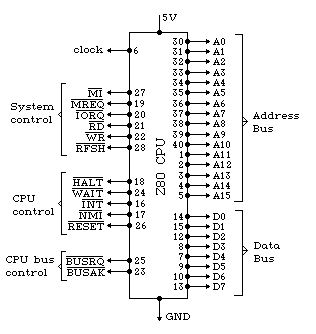
The system clock frequency just mentioned depends on the type of central processing unit (CPU, i.e. microprocessor) used in the microcomputer. Sinclair use the Z80 family: the Z80 runs at a clock frequency of 2MHz, the Z80A at 4MHz and the Z80B at 8MHz. The Z80A, which is used in all the microcomputers we’ll be considering, is housed in a 40 pin package - Fig.1 shows the connections. Some of the names used may be new to you, so we’ll briefly run through the pins and their functions. Note that the address and data bus lines are the only "active high" ones: all the rest go low (to 0V) when operative and should thus be written as RESET for example (= not reset when high, i.e. 5V). . .
The CPU generates signals on the following six lines to inform and control the other devices in the system. When the lines carry signals from the rest of the system the CPU Output is tri-state.
The remaining lines are used by the system to initiate action or to indicate that action has been taken.
Fig2. Examples of basic MOS dynamic RAM (left) and static RAM (right) memory cells. In the DRAM cell the data bit is stored as an electrical charge by the capacitor shown as 'c', in practice this is Tr2's input capacitance. The SRAM cell uses a bistable circuit for storage (Tr3/5, with Tr2/4 as loads): The cell selection lines enables data to be written in or read out. The DRAM memory cell is much simpler, giving greater storage per square area of silicon chip, but requires refreshing every 2msec. It’s not necessary to worry too much about the precise function of each of the above lines: the important thing is whether a high, low or a dynamic signal is to be expected. For instance the RESET line has to be high (except at switch on) or the CPU ceases to function. Many other lines, particularly the address and data lines, are continually changing even when the computer is apparently doing nothing. At all times the refresh system is putting out addresses and indicating their presence via the RFSH line. Although this dynamic action is rarely cyclic and often produces a meaningless pattern on an oscilloscope we shall see later that it can be turned to advantage when fault finding. Programming Knowledge After dismissing the need for a detailed knowledge of the operation of the CPU this is perhaps an appropriate time to stress the need for some knowledge of programming. Unlike other electronic systems the computer ‘s controlled by the software program and the program resident in the ROM. To expect to be able to carry out fault diagnosis without an understanding of how to program the machine is naive, and a knowledge of how the system is designed and functions can be a great help. Most home computer handbooks give instructions on programming - usually in the ‘universal’ BASIC (Beginners All-purpose Symbolic Instruction Code) language. Unfortunately however there are different BASIC systems. Sinclair BASIC is one of the most way-out, and although devotees swear by it the differences between it and others are considerable. So too are the computer start-up sequences, and it’s a great help if one knows what ought to happen when the machine is switched on. To sum up, I’d not advise anyone to attempt repairing a machine before obtaining practice and experience of its operation. More on this when we come to the ZX81 next month. Memory Chips While discussing the CPU we mentioned dynamic memories. We’d better next look at the memory family. As you probably know by now there are two basic types of memory, ROM (read only memory) and RAM (random access memory). The former are preprogrammed and non-volatile, i.e. they contain the, manufacturer’s program for operating the machine/system: this program is permanent and unchangeable. The memory in a RAM can be changed however and is used to store the data produced by the computer system. Its volatile in that all the data is lost if the supply voltage fails, but some RAMs are even more vulnerable. These are the dynamic memories (DRAMs) that require constant refreshing. With these each binary bit of every data word is stored as an electrical charge at the input of a high input-impedance transistor. This charge leaks away in about 2msec. So each bit - and there may be as many as 64K bits - has to be recharged every 2msec. A daunting task you may think. Its not quite as bad as it looks however since another feature of the dynamic RAM helps. We said earlier that sixteen address lines are required to count up to 64K, So a DRAM is going to be a multi-pin device with probably over twenty pins. In fact it has sixteen. This is achieved by matrixing the address lines. The address matrix is formed of rows and columns and a system built into the chip switches eight of the pins first to one and then the other. Externally the sixteen address lines are also switched, first to one set of eight addresses then to the remaining eight. Both these switching operations are synchronised by the CPU: the data appears on the data bus at a precise time and is read by the CPU or the memory in sync with the switching. Back to our refresh problem. The internal circuitry that does the row/column switching also assists with the refresh by recharging all the column bits each time a row is addressed. It’s necessary to refresh only the rows therefore to refresh the memory completely. The number of refresh operations is thus reduced from 64K to ~ than 256.
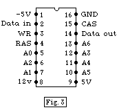
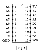
Fig. 3 shows the pin connections for the 4116 DRAM. The RAS (row address strobe) and CAS (column address strobe) pins are used to synchronise the switching. This is a 16K by one bit (serial bits enter at pin 2 and leave at pin 14) memory. Despite requiring three voltage supplies (12V at pin 8, 5v at pin 9 and -5V at pin 1) it’s still only a 16-pin device. Seven lines (A0-A6) are used for the addresses. The other pins are chassis (16) and WR (3) – read/write select. Compare this with the 2114 static RAM - see Fig. 4. Static RAMs use flip-flops to store the bits. This device has only one supply and has a 1K by four bit memory, i.e. it can store 1,024 four-bit number. Its storage capacity is a quarter of that of the 4116, yet 18 pins are required. The Z80 is an eight-bit microprocessor, these eight bits being known as one byte. It connects with an eight-line data bus and when it addresses a memory location it expects to receive an eight-bit instruction to direct its operation. The memory chips are arranged to meet this requirement: in the case of the 4116 eight of these devices would be used, providing a 16Kbyte memory; as the 2114 is a four-bit memory two of these would provide a 1Kbyte memory. When memories are assembled in this way the address lines are common to all the memory chips. If there is more than one memory group with the same address pin confusion would exist if they all unloaded their data together. To overcome this problem memories are generally provided with chip select (CS or S) or chip enable (CE) pins often more than one. These switch the memory on only when they are active. Suppose for example that four 2114 memories are paralleled on the address bus to provide 2K x 8 bits of memory. If an address in the 0-1K range is required the first two memories will be enabled whereas for an address in the 1-2K range the decoder detects the higher number (usually the next binary address line) and enables only the second memory pair. The data pins are tri-state and remain in the high-impedance state until the memory is enabled. Complete Microcomputer System
The clock oscillator for example is driven and divided automatically and the chip select signals are continually produced by the ULA logic alone. The output to the video modulator however is a complex signal consisting of screen character pixels and sync signals: the CPU is needed to sequence these correctly. The CPU and ULA also combine to carry out the keyboard decoding. Electrically the keyboard is organised in matrix form, one set of contact connections running from top to bottom and the other along the rows of keys. Signals are sequenced in the vertical lines via the ULA, a key producing a pulse on the address line. This pulse can then be decoded in a time sequence to find the key pressed. We’ve now covered the major components in this simple example of a microcomputer. But we haven’t finished with Fig. 5 because its not a fictitious example. In fact it’s a block diagram of the ZX81, the simplest Sinclair computer produced. Because of its many limitations this model has become obsolete and has little marketable value, As a result ZX81’s can be purchased second-hand for as little as Ł10 They make ideal initial practice machines. Anyone contemplating microcomputer servicing would, if he doesn’t already have a machine, be well advised to buy one of these for both the software and hardware experience. Next month well look at the ZX81 in detail and start to establish a fault-finding procedure. |
||||||||||||||||||||||||||||||||||||||||
| [ Main Page ] [ Features ] |
 The Central Processing Unit
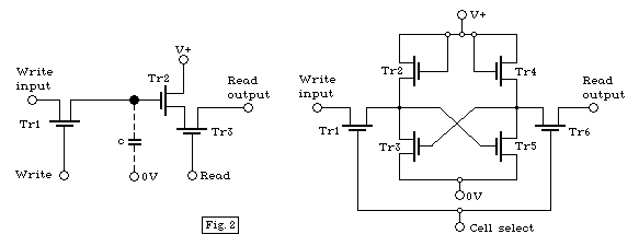
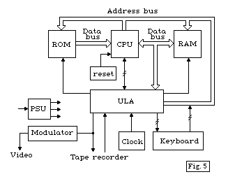 It’s time to look at the computer system
as a whole. Fig. 5 shows a block diagram for a simple computer using the
absolute minimum of components. We’ve already dealt with most of the important items
- in fact the only major item remaining is the ULA (Uncommitted Logic Army). This is a
collection of logic circuits assembled to the computer manufacturer’s specification,
replacing the many standard and special logic chips that would otherwise be required. In
this example it would provide the address decoding, produce the clock pulses, decode the
keyboard, condition the analogue tape input signals and control the output of data to the
tape recorder and video modulator. Some of these tasks are carried out by the ULA alone,
some are controlled by the CPU.
It’s time to look at the computer system
as a whole. Fig. 5 shows a block diagram for a simple computer using the
absolute minimum of components. We’ve already dealt with most of the important items
- in fact the only major item remaining is the ULA (Uncommitted Logic Army). This is a
collection of logic circuits assembled to the computer manufacturer’s specification,
replacing the many standard and special logic chips that would otherwise be required. In
this example it would provide the address decoding, produce the clock pulses, decode the
keyboard, condition the analogue tape input signals and control the output of data to the
tape recorder and video modulator. Some of these tasks are carried out by the ULA alone,
some are controlled by the CPU.