Servicing Sinclair Computers Part 4 Last month we dealt with the main parts of the Spectrum, including the CPU, ROM, ULA and 16k RAM. Fig 1 showed the main computing circuitry (issue 3 version) while Fig 4 showed the voltage stabiliser and generator circuits. Fig 5 this month completes the Spectrum circuit: it covers the tape recorder input and output and sound sections, and the video circuits. You'll find several references to Figs 1-4 in this month's article: these refer to last month's diagrams. The 32k Extension RAM Before looking at these new areas of the circuit there are a few points that remain to be dealt with concerning last month's circuitry. The first of these is the extension memory. This section, using IC15-IC26, extends the RAM memory from the initial 16k to 48k. It was originally and optional extra, with sockets provided to enable these ics to be fitted later. So you sometimes find that these ics can be easily removed for checking or for eliminating a possible source of trouble. The extension memory chips are IC15-IC22 and may be Texas TMS4532 or OKI MSM3732 chips - the memory chips must all be of the same type. These are both 64k DRAMs with only 32k of serviceable area. This area is sometimes in the range 32k to 64k. This is why there's a link panel on the printed board (between the MIC socket and the edge connector - see Fig 2 last month). The connections required for the various memory permutations are as follows:
The pin connections for these chips are shown in Fig 6, Pin 9, which is normally the A7 address connection, is here referred to as AR - high/low memory address select: it's connected to either 5V or 0V depending on whether the useful memory area is high or low. The other chips associated with the extension memory are the address decoders (IC23 and IC24) and row/column multiplexers (IC25 and IC26). The decoders activate the memory only when the A15 address line is high, thus setting the address range from 32768 (decimal) upwards.
While we're discussing addresses it's worth noting the memory map for the Spectrum. The 16k ROM starts at address zero and is followed at 16k (16384 decimal) by the 16k RAM (the 4116 chips). This continues to address 32767 and is followed by the 32k extension memory which carries on to the final address of 64k (65535). The meodel description - 16k or 48k Spectrum - indicates the size of the RAM. The 48k model often has a label on the underside. RAM Checks When you've finished a repair, especially when it has involved removing the extension memory, it's good practice to check that the entire memory is operational. This is a simple matter since one of the tasks in the initiation program is to determine the maximum usable memory available. This data is needed by the computer and is therefore stored in one of the system variables. Access is be entering the following line: PRINT PEEK 23732 + 256 * PEEK 23733 (Enter) Note that print and peek are words on the keys. The printout should be 65535, or 32767 if it's a 16k model. Any shortfall indicates that there's a memory fault that will have to be traced. If it's simply a defective memory chip diagnosis shouble be possible using the computer, because each ic is responsible for the same binary data bit at each of it's addresses. If we can find the faulty bit in the data word and we know which ic handles which bit we shall be home and dry. The above check will have told us that the faulty address, is the one beyond the printout address number. We now need to find out which bit at this address is wrong. To do whis we put 85 at this address, using the command poke. If you remember your binary you will know that 85 is 01010101. We next read what is in the address, using peek, and see if there's an error. If there is we can tell which ic is responsible because we know which data line goes to which ic (see Fig 1), We also know that D0 is the least significant digit - the one at the right-hand end - and D7 the most significant digit, the first figure on the left. So there we are. Except that an error may not show if the faulty cell registers the same digit we've put into it. In this case try again, this time putting in 170 which swaps the bits to 10101010. This must reveal the culprit.
If you don't want to exercise your binary skills, Table 1 lists the check procedure and Table 2 the faulty ic against the number read out. Remember that the system works only for a single fault at an address, though it's unlikely that there will be more than one when all the rest of the memory is operational. But there may be a fault at a higher address, so repeat the procedure until the correct final address has been obtained. Table 1 : RAM check procedures The following routine will isolate a fault at one address of the RAM: (1) Enter the following: PRINT PEEK 23732 + 256 * PEEK 23733 (2) If the result if other than 65535 or 32767 (16k version) there's a fault. (3) Add one to the faulty result. Let's say it was 54321.
Use your result +1 in place of the example quoted above. (4) If the answer returned is 85, repeat steps 3 using 170 instead of 85. (5) One of the answers should differ from the 85 or 170 entered. Provided there is only one faulty ic at the address, Table 2 will indicate which one it is. Find the line with the wrong data bit then refer to IC6-13 if the address is below 32768 or IC15-22 if the address is above 32768. (6) Repeat step 1 after the repair to ensure that there isn't another fault. Table 2 : Identifying the faulty chip
ROM Check The program given below will enable you to verify that the ROM is satisfactory. 10 LET 1=0 This will work with either make of ROM and should return the number 1926175. If "Error in Data" appears you've entered a wrong number in line 70. Incidentally if you remember that the ZX81 ROM check took over a minute to run you may be surprised at the speed of this one. Although the ROM is twice the size the check uses machine code, giving an almost instantaneous result. This is a measure of the difference between BASIC and machine code: when you consider that apart from all the addressing procedures etc over 16000 additions have been made in the time you can see the potential speed of the CPU. A connection link similar to that for the RAM is provided for the ROM. It provides for fitting a chip of either NEC or Hitachi manufacture. The link is no longer used since current ROMs work with either set of connections. The Keyboard Like the ZX81, the Spectrum's keyboard is of membrane construction wired in matrix form with decoding by the CPU. The keyboard (see Fig 5) is scanned by sequentially putting a low on each of the address lines A8 to A15 and monitoring the data lines D0 to D4. If a key is pressed the appropriate pin of the ULA chip is pulled low: this is transmitted to the relevant data line via an inverter in the ULA. Fault diagnosis is straightforward - the usual faults are in the tails that connect the membrane to the sockets. A fault here affects either a row or column of keys. It's a simple task, with aid of the diagram, to determine which tail is at fault. If the whole keyboard is dead a quick check is to make connections across from one socket to the other in place of the keyboard. This can also be done quite safely when the keyboard is removed for servicing the computer. No damage will be done even if more than one socket contact is shorted. The Spectrum Plus keyboard has an extra complication. In order to simulate the pressing of two keys by operation of one of its special keys it has a double-layer membrane. The connections between these are made by clamping the tails together, print side to print side, using a plastic clamp. This is not entirely satisfactory and can lead to some unexpected characters appearing. Replacing the Spectrum Plus keyboard is much simpler than with the earlier model however since it's assembled with screws instead of double-sided adhesive tape. Keyboards are relatively cheap and as they often take a lot of punishment it's expedient to replace any that give trouble. Tape and Sound Circuits The tape recorder input and output and the speaker are always operated independently so only one pin of the ULA is used for all three. This combined circuit also provides a sound output from the speaker when the recorder is loading. There are few components in this area and it should be a simple matter to check that the circuit is working correctly. As a guide, a 5V peak-to-peak signal at the EAR socket should give a 2V p-p signal at the ULA. With almost all such tests however the best guide is to compare the suspect signal with that in a good machine. In this particular case, if the signal is ok but there's no loading the ULA must be at fault. From bitter experience I'd recommend that you make this test before quoting for the job: the ULA is the most expensive item in the computer, costing over eight pounds at present, so it's not the sort of pricing detail to overlook. The tape output at the MIC socket should be sufficient to produce a clean recording on a standard mono tape recorder. As this level is rather low the easiest check is to save a simple one or two line program then check that it loads. Colour and Video Circuits The colour and video section is where you come into your own. At least you can work on signals you recognise, even though they are being assembled into a composite video signal rather than being decoded from it. The initial organisation of the display is carried out by the ULA, which every fiftieth of a second reads the display file - the memory area that holds the display details - and produces U, V and inverted-Y output signals. The U and V signals are fed to pins 4 and 2 respectively of the LM1889 video modulator chip IC14 which produces a standard PAL chroma output signal at pin 13. The chip incorporates a 4.43MHz oscillator which, in conjunction with external crystal network, produces phase-shifted subcarriers at pins 1 and 18. The inverted-Y output from the ULA is inverted by TR1 and added to the chroma signal at the base of TR2. The resultant composite video output is then fed to a standard Astec uhf modulator which produces an output on channel 35. If the sound output works all right but there's a problem with the display you'll need to check the circuit with a scope. One of the best points for making checks, if you have a suitable socket, is at the edge connector (see Table 3). Pin 15 on the underside of the connector is the uhf modulator's video input, pin 16 carries the inverted-Y signal from pin 17 of the ULA whiles pins 17 and 18 will carry only the sync pulses. These are positive-going and of 0.8V p-p amplitude. If a colour border, or paper, is displayed blocks appear between these sync pulses. Fig 7 shows a typical waveform but you must appreciate that the amplitude and polarity of the signal, ie whether it's above or below the sync base line, changes with the colour. With a full-screen display the inverted-luminance signal at pin 16 is a normal looking TV line signal of 2.5V p-p with no colour burst. The colour burst is very pronounced at pin 15, which carries the uhf modulator's input signal. The overall signal here is only 1V p-p however. The Edge Connector Having just referred to the edge connector, this seems a good point at which to provide the details of this output port. It's a double-sided 28-pin board-edge connector - sockets to mate with it are readily available. Every useful line in the computer is brought out to a pin and the connector provides a ready means of linking the computer to the outside world. Rather too ready at times since, as I've said before, my belief is that most of the damage to these machines occurs when devices are fitted or removed without first switching off. Table 3 : Connections to edge connector pins
Notes
Next month we'll review some of the differences between earlier and later versions of the Spectrum. |
|||||||||||||||||||||||||||||||||||||||||||||||||||||||||||||||||||||||||||||||||||||||||||||||||||||||||||||||||||||||||||||||||||||||||||||||||||||||||||||||||||||||||||||||||||||||||||||||
| [ Main Page ] [ Features ] |
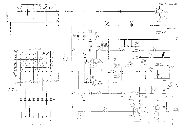
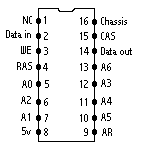 Fig.6
Fig.6 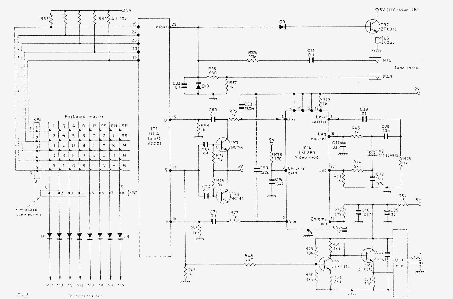